Call Us Anytime +86-591-83626970

Email Us Now sales@wts-photonics.com

banner
Home

Optical Windows

Optical Windows

  • Do you know more about optical glass Apr 24, 2019
    Speaking of glass, I think everyone is familiar with it. The windows, glasses, mirror lenses, etc. that we usually see on weekdays are made of glass. But most people may be unfamiliar with optical glass. With the continuous integration of optical and electronic information science and new materials science, the application of optical glass as the basic material of optoelectronics in the three fields of optical transmission, optical storage and photoelectric display is advancing rapidly, becoming social informationization, especially the development of photoelectric information technology. One of the basic conditions. So how much do you know about optical glass? Let's give you a knowledge of optical glass today. Optical glass is the foundation and an important part of the photovoltaic technology industry. Especially after the 1990s, with the continuous integration of optical and electronic information science and new materials science, the application of optical glass as the basic material of optoelectronics in the three fields of optical transmission, optical storage and photoelectric display is advancing rapidly. Social informationization is one of the basic conditions for the development of optoelectronic information technology. The main difference between optical glass and ordinary glass is that optical glass has high transparency, high physical and chemical uniformity, and specific and precise optical constants. Usually, the main component of optical glass, SiO2, has the characteristics of high temperature resistance, low expansion coefficient, high mechanical strength and good chemical properties. It is used to manufacture prisms, lenses, windows and mirrors with special requirements. Optical glass has a high degree of transparency and a certain quality, so its current application is also very extensive. So let's take a look at the main types of optical glass. There are six main types of optical glass, namely: ①colorless optical glass ②colored optical glass ③ radiation-proof optical glass④radiation-resistant optical glass⑤ultraviolet and infrared optical glass ⑥optical quartz glass. After this science, do you know more about optical glass,Optical Glass Cylindrical Lenses,Optical Glass Penta Prisms? If you are interested in optical glass, please contact us!
  • Optical analysis method Dec 20, 2018
    Optical analysis method Optical analysis method is a kind of analysis method based on the interaction between the light radiation energy and matter (luminescence, absorption, scattering, photoelectron emission, etc.).It belongs to a kind of important method in instrument analysis, which can be divided into two kinds: spectral method and non-spectral method.Spectral analysis is based on the measurement of the internal relation between the energy of light radiation and the composition and structure of matter and its manifestation, spectrum (or spectrum).Non-spectral analysis, which does not include changes in the internal energy of matter, but based on changes in radiation direction and physical properties caused by matter. Spectral method can be divided into three basic types: 1. Luminescence spectroscopy Including atomic emission spectrometry, atomic fluorescence spectrometry, molecular fluorescence analysis, X-ray fluorescence analysis, electronic energy spectrum analysis. 2. Absorption spectroscopy Including uv spectrophotometry, infrared spectrophotometry, electron spin resonance and nuclear magnetic resonance spectrometry, musball spectrometry, atomic absorption spectrometry, etc. 3. Scattering spectrum method The main method is Raman scattering spectrum.Non-spectral methods include refraction, polarization, rotatory dispersion, circular dichroism, X-ray diffraction and turbidity analysis.
  • Manufacturing principle of optical glass pressure type Sep 21, 2018
    The forming process of optical blank is directly related to optical glass melting technology and optical processing technology.So you have to think about them as a system in general. Since the development of optical glass, glass parts blank (lens, prism) production is generally will be melted good chunk glass material, to soften, loading metal mold pressing into the shape of the roughly, and then through the coarse grinding, fine grinding, polishing and make out.This method was used as an auxiliary method after the appearance of optical glass continuous melting technology in the 1970s Since the 1970s, the main factories in Japan with developed optical glass have adopted the most advanced production technology in optical glass production.Three straight (3 D) production technology, namely direct electric melting, molding, precision directly annealing directly, including direct forming continuous melting or crucible leakage drops of material forming method, abroad to be called "pressed" at a time.This kind of advanced forming technology is the glass directly compressed into optical blank, so that greatly simplify the production technology of secondary molding, saves the manpower, equipment, reduce energy consumption, improve the utilization rate of raw materials.Japan's valley company three straight line optical glass, the clay crucible furnace classical method need to 170 days, with platinum crucible pouring method need to shorten the production cycle of 34 days to 3 production cycle.The yield increased from the highest 40% in classical law to more than 90%. 
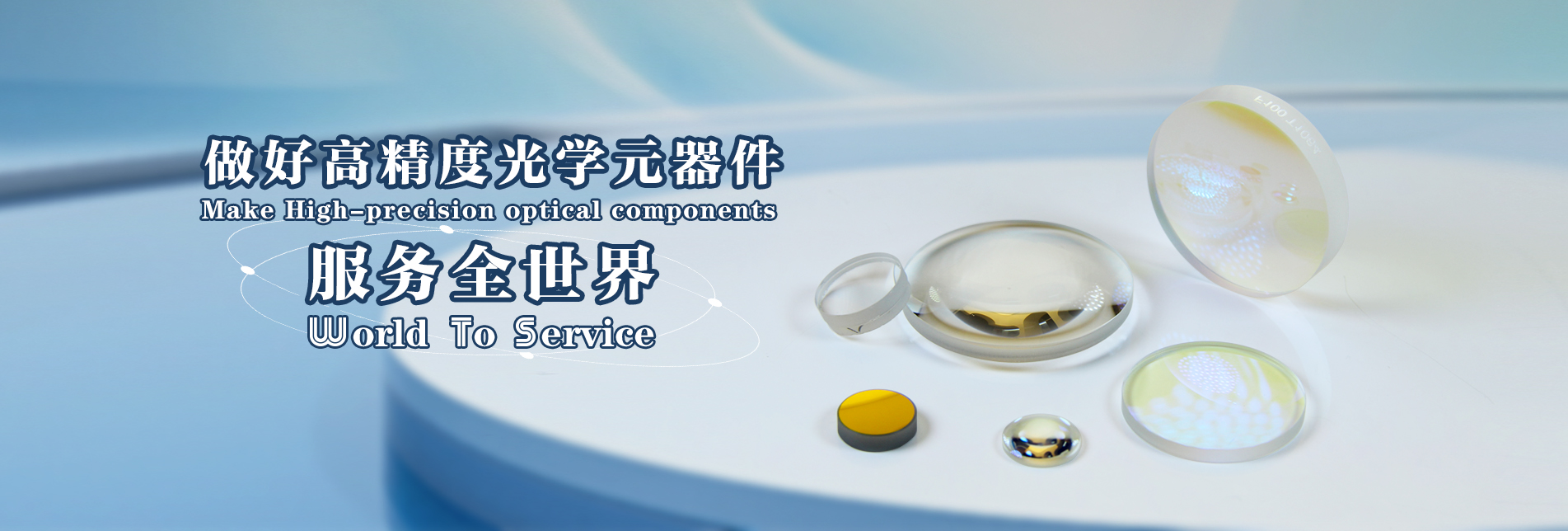
The optical glass pressing type is also called non-abrasive pressing type, which means that the optical elements produced by the pressing type do not need grinding, polishing, grinding edge, center and other optical processing, and are directly assembled to the optical instrument.The optical glass molding pieces of surface finish and dimensional accuracy requirements quite high, usually with optical gauge block on the optical element surface finish and dimensional accuracy measure, measure its quality to produce the number of interference fringes, for lens for the camera systems usually require through the lens radius of Newton ring number should be less than 6, through the two mutually perpendicular radius of the number of Newton ring sent to less than three, two kinds of Newton ring number is less, the higher the quality of the lens. Precision pressing involves placing heated and softened glass into a mold protected by an inert gas, such as nitrogen 2, which has a high surface finish and dimension precision on its inner surface.Attached to the inner surface of the material should have high hardness, good oxidation resistance, good thermal conductivity, not bonded with glass at high temperature, good impact strength and analysis strength, not through the gas, water vapor and liquid.The materials that meet the above requirements are glass carbon, silicon carbide and silicon nitride.However, compared with the latter two, the glass carbon is loose and easy to oxidize, easy to scratch and small elastic modulus.Low impact and analysis strength, poor thermal conductivity.According to foreign patent reports, glass carbon was used on the inner surface of the moulding mould in the early 1970s, while silicon carbide or silicon nitride was used in patents issued in the mid-1970s.The methods to attach the two materials to the inner surface of the mold include (1) hot pressure, (2) ion splash lining and (3) gas deposition.The thickness of its fixation layer is at least lOptm.The structure of this kind of mould is quite complex. After the glass pressing is finished, the mould cannot be removed immediately, and the glass temperature needs to be lowered below the transition temperature before it can be removed.Precision pressing can suppress the optical parts of the sphere, aspheric surface and other complex shapes.In the mid 80 s to the production of optical glass is made of moulded a forming two precision lens of glass surface machining precision of Y / 10, 10 um thickness and diameter tolerance, wedge Angle is less than 10-3 mil., birefringence per CM less than 10, Y/refractive index evenness of 10-6, a precision molding precision lens in Japan, Germany and other countries have adopted. The production of optical glass has gone through the development process of lump material and secondary pressing material and direct liquid pressing material.At present, the main supply form of optical glass production in China is still lump material.Considering the economic benefit of the whole optical industry, it is urgent to develop the production of type materials.Based on China's current optical glass production technology level and the actual needs of the market, we should first do a good job of secondary pressure production, in the improvement of secondary pressure production to pay attention to the solution of good material preparation.Mold release agent, non-stick glass over porcelain box materials and mechanical f {2 son main technology problems, such as automation, direct liquid pressure type a secondary pressure type for obvious technical and economic effect, is the only way for optical glass production in the future.But starting from the actual needs of the current optical industry in China and at the same time refer to the international development trend of the optical glass production technology, the developing direct liquid pressure type it is important to pay special attention to the development of our country many varieties, small batch of many specifications of pressed directly, and to solve the good small batch direct optical glass molding must first solve the small batch optical glass melting technology, development of the corresponding optical glass melting tank furnace.While developing and improving the secondary pressure type and direct liquid pressure type, the research and test of precision pressure type should be carried out actively so that China's optical glass pressure type technology can catch up with the world advanced level as soon as possible.
  • What is a Prague mirror? Aug 03, 2018
    Bragg reflector (also known as distributed Bragg reflector) is a reflector structure consisting of two optical materials composed of adjustable multilayer structures.The most common is a quarter mirror, with each layer of thickness corresponding to a quarter of the wavelength. Bragg reflector (also known as distributed Bragg reflector) is a reflector structure consisting of two optical materials composed of adjustable multilayer structures.The most common is a quarter mirror, with each layer of thickness corresponding to a quarter of the wavelength.The latter condition applies to the case of direct incidence. If the reflector is used for the case of a large Angle of incidence, the relative thickness of the required layer is larger. How the Prague mirror works Fresnel reflections occur at each interface of the two materials.At the working wavelength, the distance difference between the reflected light at the two adjacent interfaces is half a wavelength. In addition, the symbol of the reflection coefficient at the interface will also change.Therefore, all the reflected light at the interface will interfere with each other and get strong reflection.Reflectivity is determined by the number of layers and the refractive index difference between materials.Reflection bandwidth is mainly determined by refractive index difference. FIG. 1 shows the electric field penetration curve of Bragg reflector with 8 layers of TiO2 and SiO2 materials.The blue curve corresponds to the intensity distribution of light with a wavelength of 1000nm coming in from the right.It should be noted that the intensity curve outside the mirror oscillates due to the interference effect of waves in the opposite direction.The gray curve is the intensity distribution curve when the wavelength is 800nm, when a large part of the light can pass through the reflector coating. The electric field penetration curve of the Bragg mirror. Figure 2 shows the change curve of reflectivity and group time-delay dispersion with wavelength.Reflectivity is very high in some optical bandwidth, which is related to the refractive index difference and layer number of materials used.Dispersion is calculated by the second derivative of reflected phase with respect to optical frequency.Dispersion is small at the center wavelength of the reflector band, but increases rapidly on both sides. Figure 3 shows the color scale of the optical field penetrating reflector.As you can see, only a small fraction of the light field can penetrate the reflector. The type of the Bragg mirror Bragg reflectors can be prepared by the following techniques: Dielectric reflectors employ thin-film coating techniques, such as electron beam evaporation or ion beam sputtering, which can be used as laser reflectors for solid-state lasers. This reflection consists of amorphous materials. Fiber Bragg gratings, including long-period fiber gratings, are commonly used in fiber lasers and other fiber optic devices. Similarly, the body Bragg grating can also be made from photosensitive materials. The semiconductor Bragg mirror can be prepared by photolithography. The reflector can be used in laser diodes, especially in surface-emitting lasers. There are also various kinds of Bragg reflectors used in waveguide structure, which adopt corrugated waveguide structure and are prepared by photolithography. This type of grating can be used in some distributed Bragg reflectors or distributed feedback laser diodes. There is also a multi-layer reflector design, which is different from the simple one-fourth reflector design. With the same number of layers, it usually has a lower refractive index, but can be optimized as a dichroic reflector or chirped reflector for dispersion compensation.
  • How to input the data measured by interferometer into OpticStudio Jul 06, 2018
    In this case we use ZYGO interferometer provide data as example, ZYGO interferometer generated data file format for company. ZXGRD file, we need in OpticStudio converts the file format. DAT file. We use ZYGO interferometer provide data as example, ZYGO interferometer generated data file format for company. ZXGRD file, we need in OpticStudio converts the file format. DAT file, and to save the file in Zemax root directory "DocumentZemax/ObjectsGrid Files". The screenshot at the beginning of the data file shows that the data format is the same as the Grid Sag data format mentioned in last week's article.The number of data points in XY direction is 732, and since the distance between data points is 0.01344, the diameter of the data file is 9.72mm.Where the first line of the file has a terminal flag (flag) of 0, representing the data unit of mm. It should be noted that if the measured data is stored as wavefront data, we need to treat this data file as phase data.The Grid Sag of OpticStudio is in radians.Therefore, the measurement data need to be converted, and the conversion formula is as follows: Zemax unit (radian) = ZYGO measurement unit (mm) x 2 In the data file provided by this example, the measured wavelength is 632.8nm, then: Zemax unit (radians) = ZYGO measurement unit (mm) x 2 PI / 0.0006328 = 9924 x (ZYGO measurement unit) In aperture lens editor (STO) phase surface type set to a grid, and properties on the surface - the import TAB in the previously saved data file to import, in this case for the test. The DAT file, as shown in the figure below. Meanwhile, the Diffraction order of Grid Phase is input with the unit conversion value calculated above: Click ok to see the following interferogram results, which are consistent with the data on the interferometer.
  • How does Opticstudio sample in wavefront calculation Jun 22, 2018
    How to sample in Wavefront based analysis and calculation, including Wavefront Map, point spread function (PSF) and modulation transfer function (MTF). Question: Where is the center of the sampling grid in the wavefront graph and other correlation analysis? First of all, we observe the wavefront figure, wavefront data is the foundation of many other OpticStudio analysis functions, such as PSF, MTF and circle into Energy (Encircled Energy). When doing numerical calculations, we want to maintain the symmetry of the pupil and keep the position of the main light at an actual point in the middle of the beam.Also, we need to determine a central point for the FFT algorithm.In order to fulfill these requirements, we need to define the center of the pupil in the pupil space (called by different definitions the near field or space field), namely (n/2+1,n/2+1).So when you look closely at the wavefront diagram you see that the data in the leftmost column is all zero. So let's look at the PSF analysis.PSF is the result of the wavefront square after the fast Fourier transform.The FFT PSF We can see that the PSF is centered around the pixel in (n/2,n/2), which is the pixel in (16,16).This is related to the way FFT is calculated and the definition of direction in OpticStudio.When the center point of the grid is n/2+1 in one domain (such as the spatial domain), the center point coordinate in another domain (such as the frequency domain) is n/2.A close look at the figure below shows that the data in the left-most column and the bottom row are blank. In MTF calculation, MTF is the autocorrelation function of wavefront, and the number of pixels is usually twice that of the wavefront graph (regardless of the change of coordinate axis).Therefore, for the sake of MTF, OpticStudio will first supplement 32x32 data points to 64x64 data points with data 0, and then conduct self-correlation calculation.For the 3d FFT MTF (Surface FFT MTF), OpticStudio will square the FFT before the wave, and then calculate its FFT. In other words, MTF is the Fourier transform of PSF. We get the following results: You can see that the peak point is at the coordinate (32,32), or at (n/2,n/2). OpticStudio determines the frequency interval of 3d FFT MTF by using the boundary of the autocorrelation function 1/(lambda*F/#), where lambda is the shortest wavelength in the system (if we calculate the multi-wavelength result).OpticStudio actually calculates the cutoff frequency of all wavelengths multiplied by the number of F's, and scales the entire chart based on their maximum results.Other wavelengths are scaled in the pupil space to allow all PSF to sample at the same distance.To double cutoff frequency can be the width of the optical transfer function (OTF) (above the graph 850.06 cycles/mm), then the results divided by 2 * n (MTF calculating the number of pixels after zero padding) get sample point spacing. For example, the width of OTF is 850.06 cycles/mm, and the sampling point is 32x32.So the point spacing is 850.06/64 = 13.282 cycles/mm.The center point of the 3d FFT MTF graph is located at the coordinate (n/2,n/2)=(32,32), and the corresponding frequency is 0 in the graph.In other words, the 32nd column pixel corresponds to a point on the X-axis with a frequency of 0 cycles per mm.Column 33 corresponds to a space frequency of 13.282 cycles/mm, column 34 corresponds to a space frequency of 26.564 cycles/mm, and so on.The last column, column 64, has a corresponding spatial frequency of 32*13.282 = 425.03 cycles/mm.The first column corresponds to a space frequency of -31*13.282 = -411.748 cycles/mm. As with PSF, 3d FFT MTF charts have left-most column and lower-most behavior white space data.Therefore, the data on the left and right sides of the frequency coordinate axis is not strictly symmetric (the same is true for the top and bottom sides).But keep in mind that each data is symmetric along the "center" of the frequency coordinate system.If you consider a "half-cell pixel" on the left or right (up or down) edge, the entire width is indeed 850.06 cycles per mm.The edge of a finite size pixel covers the entire width, but the central coordinates of each pixel (per column or row) are inserted by half a pixel from each side. We wholesale a variety of aspherical optical components, including Optical precision glass aspheric lenses,Precision Aspheric Lenses and more.
  • Aspheric Optical Element Profile Detection Method Jun 06, 2018
    With the development of science and technology, sophisticated products and modern weapons are increasingly demanding quality of optical element, aspheric optical element because of excellent performance and application is more and more widely, demand more and more urgent, aspheric component surface shape detection researchers have become the focus, the paper focuses on the existing aspheric optical element face detection method, this paper introduces the principle of detection of various methods and the advantages and disadvantages of various methods is presented. Aspheric and closest to the sphere along the normal direction of the deviation vector, said curve OP0A for aspheric surface, curve OM0A is closest to the sphere, C is the most close to the sphere centre, curve OP0A 'is and nearly spherical concentric and tangent to the aspheric sphere, POMO is the largest non sphericity.The maximum value of non-sphericity is an important basis for processing and testing.In the testing of aspheric components, how to measure the aspheric surface forms found in the most close to the reference surface deviation vector, and then the design value compared with the most close to the reference spherical differential, compute the closest with aspheric reference spherical difference compared to calculate and closest to the reference spherical surfaces is the steradian, at various points in the curvature radius and is an important part of the ball into testing. We wholesale a variety of aspherical optical components, including Optical precision glass aspheric lenses,Precision Aspheric Lenses and more.
  • The Application Principle Of Optical Coating Is Briefly Described May 31, 2018
    Principle of membrane interference 1.The fluctuation of light. The wave-particle duality of light is known to be the same as radio waves and x-rays.The rays are electromagnetic waves, but they have different frequencies.The relationship between the wavelength of electromagnetic wave, frequency u and propagation rate V is as follows: V = lambda u Since electromagnetic waves of various frequencies travel at equal speed in a vacuum, they have different wavelengths.High frequency with short wavelength and long wavelength.For comparison, can according to the radio waves, infrared, visible light, ultraviolet rays, X rays, and gamma rays, the size of the wavelength (or frequency), such as put them in turn arranged in a spectrum, the spectrum of electromagnetic spectrum. In the electromagnetic spectrum, the longest wavelength is the radio wave, which is divided into long wave, medium wave, short wave, ultrashort wave and microwave due to the different wavelength.The second is infra-red, visible and ultraviolet light, which are collectively called light radiation.Of all the electromagnetic waves, only visible light can be seen by the human eye.The wavelength of visible light is about 0.76 microns to 0.40 microns, which is only a small part of the electromagnetic spectrum.Again, x-rays.The shortest wavelength of electromagnetic waves is y rays. Since light is a kind of electromagnetic wave, it should be realized in the process of transmission, such as interference, diffraction, polarization and so on. 2.Thin-film interference The film can be a transparent solid, liquid or a thin layer of gas sandwiched between two pieces of glass.The incident light reflected thin film on the surface after the first beam of light, reflection, refraction of light through the film surface and after surface refraction on the second beam of light, the light on the same side of the membrane, separated by the same incident vibration, is a coherent light, belongs to the amplitude of interference.If the light source is an extended light source (surface light source), the interference can only be observed in the specific overlapping area of the two coherent beams, so it is a localized interference.The two surfaces are parallel to each other, and the interference fringes are infinitely far away, usually by means of convergent lens in their image.For the wedge film, the interference fringes are localized near the thin film. Both experiments and theories have proved that interference fringes can be produced only when two light waves have certain relations, which are called coherence conditions.The coherence conditions of the film include three points: the frequency of the two beams is the same;The beam of light waves vibrates in the same direction.The phase difference between two light waves remains constant. The optical path difference between the two coherent light interfered by thin film is: Δ=ntcos(α)±λ/2 Where n is the refractive index of the film;T is the thickness of the film at the incident point;Q is the refractive Angle in the film;Direction /2 is the additional optical path difference caused by the reflection of two coherent beams of light at two interfaces of different properties (one is the optical defiled medium to the optical dense medium, the other is the optical dense medium to the optical defiled medium).The principle of thin film interference is widely used in optical surface inspection, precise measurement of small Angle or linearity, preparation of anti-reflection film and interference filter. WTS Photonics Co.,Ltd is optical lenses factory,optical products supplier. Optical products includes optical windows,optical lenses,optical prisms etc. Fused silica windows,optical glass achromatic lenses,right angle prisms are important services here!
  • Din3140 surface quality standard May 17, 2018
    ★ 1/1x0.04, 1/1 x 0.04 allow a bubble with a diameter of 0.04. In fact, the area of the bubble is: 1 x 0.042=0.0016mm2 can be divided into many small bubbles, but its total area is the same.If: 1/1 times 0.04 is the same as 1/3 x 0.025 or 1/6 * 0.016,1/16 * 0.001 etc. If the expression has parentheses, it cannot be broken into multiple small bubbles. ★ 2/01 2/ denotes the requirement of stripe, 2/01 indicates that the band 01 is allowed to be 01~04. ★ 3/3 (1) 0.5 3 / said demand for aperture 3/3 f number is 3, (1) 0.5 said Numbers in brackets in the two vertical direction f number difference, that is, a direction of aperture is 3, 2 vertical aperture for local error (smooth on the interference fringes of minor deviations) allow 0.5 a circle ★ 4/3.2 '4/ indicates the demand for eccentricity of 4/3.2' indicates that the surface inclination is 3.2 ', for example, the amount of eccentricity at the center of the ball is calculated as C: C= surface inclination x spherical radius /3438 cases: R=53.43 surface inclination 3.2 ', C=3.2 * 53.43/3438=0.0497mm. ★ 5/1x0.063; K2 x 0.004;R0.1 5/ represents the requirement for surface defects 5/1 * 0.063;K2 x 0.004;R0.1 1 x 0.063 indicates that a hemp point with a size of 0.063mm is allowed, which can be converted into a lot of small hemp points, such as: 1 * 0.0632=0.004mm2, which can be converted into the following: 3 * 0.05;6 x 0.025;16 * 0.016;40 x 0.010 can be converted to: 1 * 0.04+4 * 0.025, as long as the total area of the hemp is kept unchanged, with parentheses, it cannot be broken up into multiple small pitts.K2 x 0.004 indicates that the scratch marks of two arbitrary lengths with a width of 0.004mm can also be removed into many small scratches with the same scratch area, but the total area remains the same.The scratch area can also be replaced by a pitting area.R0.1 indicates that there is no limit to the number of broken edges with a depth of 0.1mm. ★ 50/2 x 0.1;G2 x 0.25;C2 * 0.25 50/ indicates the requirement for surface defects of the film after coating is 50/2 x 0.1;G2 x 0.25;C2 * 0.25 indicates that the film layer allows two defects with a size of 0.1mm (including pitting and scratches, etc.), as well as two gray patches with a size of 0.25mm and a color spot of 0.25mm. ★6/10 indicates that the requirement for material stress is 6/10, which means that the optical path difference of 10nm is allowed, that is, the light is allowed to produce a difference of 10nm after every 1cm.
  • WTS Lets You Understand 9 Optical Films(Coating ) Apr 23, 2018
    Optical films are ubiquitous in our lives, from precision and optical devices and display devices to optical film applications in everyday life; Optical films can be classified according to their use classification, characteristics and applications: reflective film, anti-reflection/anti-reflective film, filter, polarizer/polarizer film, compensation film/phase plate, alignment film, diffusion film/sheet, Brightening film / prism sheet / condenser film, shading film / black and white glue. Related derivatives include optical grade protective films, window films, and the like. 1. Reflective films can generally be classified into two types, one is a metal reflective film, and the other is an all-electric reflective film. 2.Anti-reflection / anti-reflection film Anti-reflection coating, also known as anti-reflection coating, its main function is to reduce or eliminate the reflected light of the lens, prism, plane mirror and other learning surfaces, thereby increasing the light transmission of these components, reducing or eliminating the system's stray light. 3, Filter Filters are made of plastic or glass and then add special dyes, red filters only allow red light to pass, and so on. The refractive index of the glass sheet is almost the same as that of air, and all shades can pass through, so it is transparent, but after the dye is dyed, the molecular structure changes, the refractive index also changes, and the passage of certain colors of light changes. For example, when a white light passes through a blue filter, it emits a beam of blue light. The green and red light are very few and most of them are absorbed by the filter. 4.Polarizer The full name of the Polarizing Film should be a polarizer. The main role of the polarizer is to make the non-polarized natural light become polarized, converted into polarized light, plus the torsional characteristics of the liquid crystal molecules, to control the passage of light, thereby increasing the transmittance and viewing angle range, forming Anti-glare and other functions. 5.Compensation film/phase difference board The compensation principle of the compensation film is to correct the phase difference produced by the liquid crystals at various viewing angles in various display modes (TN/STN/TFT (VA/IPS/OCB)). In brief, it is the birefringence of liquid crystal molecules. The nature is compensated for by symmetry. 6, the alignment film The alignment film is a thin film with straight stripe scratches, and the role is to guide the arrangement direction of the liquid crystal molecules. 7, the proliferation of film The diffusion film is a key component of the TFT-LCD backlight module and can provide a uniform surface light source for the liquid crystal display. 8, Brightness enhancement film / prism sheet / condenser film Brightness enhancement film is also called Prism Sheet, often abbreviated as BEF (Brightness EnhancementFilm), and is a key component in the TFT-LCD backlight module. It is mainly based on the principle of light refraction and reflection. 9, Shading film / black and white glue Black and white shading glue | shading film is mainly used in the backlight source, from the fixed, shading effect (cover off the side light and light position of the light), also known as shading film, black and white film, referred to as black and white glue (can be said to be a kind of double-sided tape) . Through this knowledge shared by WTS, we have a better understanding of these membrane systems. Our company also has AR film, MgF2 film, AL film (metal film) Optical Windows,Optical Lenses,Optical Prisms,products. Welcome inquiry.
WTS PHOTONICS CO.,LTD was founded in 2009 and was awarded the National High-tech Enterprise in 2021, the Fujian Provincial Science and Technology Little Giant Enterprise, and the Fujian Provincial Profession Precision-Specialization-Innovation enterprise in 2022. WTS locate in the beautiful southeast coastal city, Fuzhou, a famous optical city in China.   WTS has 11,000 square meters of standardized factory buildings, a group of skilled technical staff, and a complete optical processing system, coating system, assembly system, and quality control system. WTS provide customers with one-stop solutions for R&D, design, and manufacturing of high-precision optical components, high-precision optical imaging lenses, and high-power laser components. WTS‘s products include optical windows, lenses, cylindrical lenses, filters, mirrors, prisms, waveplates, beamsplitters, laser crystals, lenses assembly and module etc. Products are widely used in machine vision, industrial lasers, biomedicine, precision instruments, aerospace, AR&VR, Semi-Conductor, ADAS, Vehicle Optics and optical communications.   WTS are certificatied by ISO9001, ISO14001, ISO13485 and IATF16949. WTS have been deeply involved in optics industry for tens of years and service customers around the whole world. Based on quality, drived by technology, talent is future, WTS Continuously developing and innovating, achieved excellent quality and reputation.
facebook linkedin twitter youtube
Contact Us
BUILDING 16#, NO.20 ZHIHUI ROAD NANYU TOWN MINHOU COUNTY, FUZHOU, CHINA

Copyright @ 2025 Fuzhou WTS Photonics Technology Co., Ltd. All Rights Reserved. Network Supported

Sitemap / Blog / Xml / Privacy Policy

Leave A Message

Leave A Message
If you are interested in our products and want to know more details,please leave a message here,we will reply you soon. email: sales@wts-photonics.com
Submit

Home

Products

whatsApp

contact